
High Purity Metal For Sensitive Electronic Devices
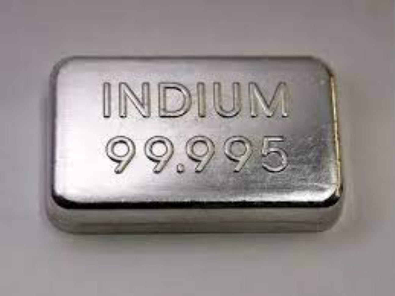
High Purity Indium Metal
Description
High Purity Indium 5N 6N 7N 7N5, is a soft, silvery-white, light blue luster and malleable ductile solid with atom weight 114.818, melting point 156.61°C and density 7.31g/cm3, which is react with the oxygen in the air slowly to form thin layer of oxidation film. High purity Indium are available 99.999%, 99.9999%, and 99.99999% in size of bar, ingot, stick granules, and sheet etc.
Applications
High Purity Indium is primarily used in the manufacturing of III-V compound semiconductors indium antimonide InSb, indium arsenide InAs, indium phosphide InP, and indium nitride InN for ultra-high efficiency photovoltaic solar cells, photoconductors, infrared detectors, infrared LEDs, high-speed data lasers, electronic switching applications, high purity alloys, electronic paste, transistor base, ITO powder and target for LCD, as well as the source material for semiconductor epitaxial growth using LPE, CVP and MBE method, and as the dopant of germanium and silicon single crystal growth etc.
Delivery
High Purity Indium 5N 6N 7N 7N5 (99.999%, 99.9999%, 99.99999% at Jaytee can be delivered in in size of bar, ingot ,stick granules, and sheet etc . Indium products in different grades are in package of composite aluminium coated poly begs bag with carton box outside or may be customized packaging.
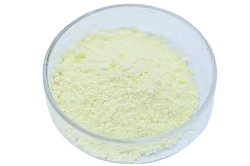
High Purity Gallium
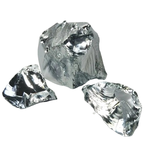
Description high-purity-gallium
High Purity Gallium, 99.999%, 99.9999% and 99.99999% 5N 6N 7N, soft metal, silvery white in liquid state and bluish white in solid state, atom weight 69.723, melting point 29.76°C and density 5.91 g/cm its erosion almost not affected by oxygen and water at room temperature, is oxidized only at high temperature.
Applications
High Purity Indium is primarily used in the manufacturing of III-V compound semiconductors indium antimonide InSb, indium arsenide InAs, indium phosphide InP, and indium nitride InN for ultra-high efficiency photovoltaic solar cells, photoconductors, infrared detectors, infrared LEDs, high-speed data lasers, electronic switching applications, high purity alloys, electronic paste, transistor base, ITO powder and target for LCD, as well as the source material for semiconductor epitaxial growth using LPE, CVP and MBE method, and as the dopant of germanium and silicon single crystal growth etc.
Delivery
High purity Gallium 99.999%, 99.9999% and 99.99999% 5N 6N 7N can be delivered in form of container shape of 100g, 500g or 1000g weight, which is packed for safety and suitable transportation with dry ice box.
High Purity Tin
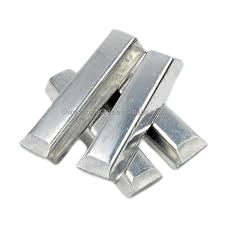
Description
High Purity Tin Sn 5N 6N 7N is a silvery white glossy soft and odorless solid metal with atomic weight 118.71, density 7.29 g/cm3 and melting point 231.88°C. High purity tin can be purified into bar, ingot and shot by the purification process of refining and zone-floating technique to 99.999%, 99.9999% and 99.99999% level for many exciting applications.
Applications
High purity Tin metal is widely used in manufacture of compound semiconductor, high purity alloy, superconducting material, solder and as a dopant of compound semiconductor
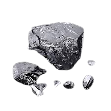
High Purity Antimony
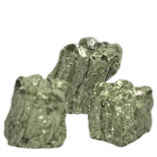
Description
High Purity Antimony Sb 4N5, 5N, 6N, 7N, 7N5, a silver white brittle and crystalline metal, atomic weight 121.76, density 6.62g/cm3, melting point 630°C, boiling point 1750°C. High purity antimony is obtained to more than 99.995%, 99.999%, 99.9999%, 99.99999% and 99.999995% purity by purification method with multistage vacuum distillation, zone melting process or single crystal pulling growth techniques etc. High Purity Antimony 5N 6N 7N 7N5 Sb qualified by ICP-MS or GDMS at Western Minmetals (SC) Corporation can be delivered in various forms of irregular lump 3-25mm, shot 2-6mm, bar D20-40mm, and D15-25mm crystal for MBE application.
Delivery
High Purity Tin Sn 5N 6N 7N with purity of 99.999%, 99.9999% and 99.99999% can be delivered in size of lump, chunk, shot, ingot 500g or 1000g, bar and crystal. Tin products in various grades are packed in coated poly bag with carton box outside or may be customized packaging.
Applications
High Purity Antimony Sb is used for the preparation of high purity alloy, diodes, electronic refrigerating elements, film for optical memory disk, thermo-electron converter, photovoltaic, and infrared materials sectors, as well as a dopant in n-type semiconductor silicon and germanium monocrystal. High purity Antimony is important source metals for growing crystals of III-V compound semiconductors like Indium antimonide InSb, gallium antimonide GaSb and bismuth antimonide BiSb used for Hall sensors and infrared detectors, and as epitaxy source for MBE growth with various forms and shapes.
Delivery
High Purity Antimony 5N 6N 7N with purity of 99.999%, 99.9999% and 99.99999% can be delivered in size of lump, needles, powder, shot, ingot 500g or 1000g, bar and crystal. Antimony products in various grades are packed in coated poly bag with carton box outside or may be customized packaging
High-Purity Indium -Tin oxide
The high-purity indium tin oxide (ITO) is transparent conductive oxide which is used in semiconductor industry specially in optoelectronic devices. ITO is known for its unique tin and indium oxide combination of high electrical conductive and optical transparency, making it useful in modern technology.
Properties
1.Electrical Properties:
✓ High Electrical Conductivity: ITO is excellent electrical conductivity, material which allows it to act as a conductive layer in electronic devices.
✓ Low Resistivity: High-purity ITO has low resistively, which is crucial for applications requiring efficient electrical performance.
2.Optical Properties:
✓ High Transparency: One of ITO’s most notable properties is it has optical 80-90% transparency in visible light range. This makes is ideal for applications were conductivity and visibility are required.
✓ Wide Bandgap: ITO has a wide bandgap, which contributes to its transparency in visible light while still allowing for electrical conductivity.
3.Mechanical Properties:
✓Thin Film Application: ITO applied as a thin film which is mechanically flexible to some extent, depending on the thickness of the film and the nature of the substrate.
Applications
1.Display
- ✓As a transparent conductive layer in liquid crystal displays (LCDs).
- ✓As a anode layer organic light-emitting diodes (OLEDs).
2.Touch screens
- ✓ As a transparent conductive layer is capacitive touch screens.
3.Solar cells
- ✓As a transparent conductive layer in tin film photovoltaics.
4.optoElectronics devices.
- ✓ As a optoelectronic devices for sensors and light modulators.
High-Purity Silicon Metal
Jaytee has the techniques to achieve the high purity of silicon metal 99.9999% (6N). This high-purity silicon is used primarily in the semiconductor industry to produce single crystal silicon wafers, which are critical for the fabrication of semiconductors devices and operate reliably and efficiently, as even minor levels of impurities can significantly affect performance.
Properties
✓Semiconducting Property: Silicon has bandgap of approximately 1.1 eV, which allows it to conduct electricity under certain conditions. These properties of silicon make suitable for semiconductor industries.
✓Doping ability: High-purity silicon has the ability of doping with boron family and nitrogen family elements to create p-type or n-type semiconductor respectively.
✓Crystalline Structure: High-purity silicon single crystal has cubic diamond lattice structure which are used in semiconductor industries.
✓Thermal Conductivity: Silicon also has good thermal conductivity, to manage heat flow in electronic devices.
✓Silicon Wafers:Silicon wafers, which are slices of single-crystal silicon, are brittle but can be very thin and precisely manufactured for use in semiconductor devices.
Applications
1.Silicon Wafers:
✓Substrate Material: High-purity silicon wafers are the foundational substrates for most semiconductor devices. These wafers are sliced from a single-crystal silicon boule and are used as the base on which electronic circuit are fabricated.
2. Integrated Circuits (ICs):
✓Microprocessors and Memory Chips: High-purity silicon is used to manufacture ICs, which are essential components in computers, smartphones, and various electronic devices.
3. Solar Cells:
✓Photovoltaic Cells: Silicon wafers are also used in solar cells to convert sunlight into electrical energy. High-purity silicon improves the efficiency of photovoltaic cells.
4. Sensors and Devices:
✓Semiconductor Sensors: High-purity silicon is used in various sensors and devices, including temperature sensors, pressure sensors, and other electronic components.
JAYTEE ALLOYS CAN SUPPLY BULK QUANTITIES OF HIGH PURITY METALS FOR SENSITIVE ELECTRONIC DEVICES AT BEST POSSIBLE RATES. IT CAN ALSO MANUFACTURES VARIOUS KINDS OF HIGH PURITY METALS FOR SENSITIVE ELECTRONIC DEVICES AND CAN SUPPLY AS PER CUSTOMER REQUIREMENT. KINDLY CONTACT US FOR MORE INFORMATION.
Contact Us